
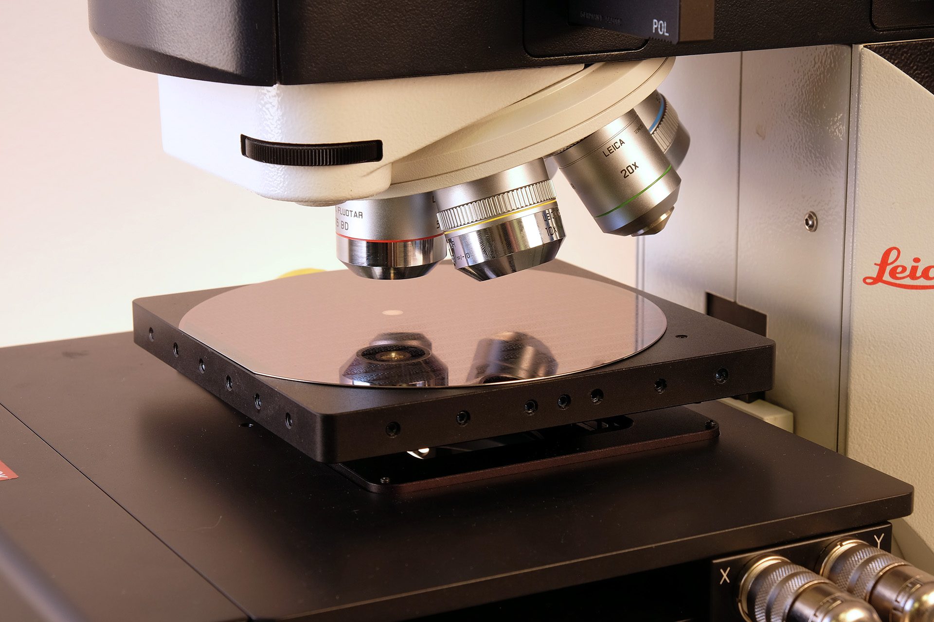
Advances in laser grooving means that manufacturers are able to optimize die separation quality by combining traditional blade dicing and laser grooving techniques to separate individual chips from the silicon wafer. However, it is still a costly use of time as the groove must be visually inspected by a microscope operator, which also introduced individual dependencies. Using Vision PE microscopy system, Clemex has demonstrated a new automated process that reduces the technician time spent analyzing the die, at the same time improving the accuracy of the measurement.
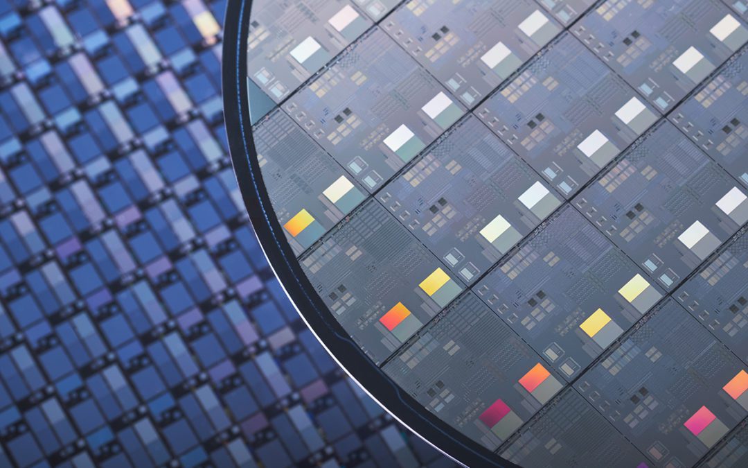
 Ever since silicon wafers have been setup to accommodate multiple dies, there has been the problem of the safe and uniform removal of the dies. The traditional technique has been to use an extremely sharp blade to saw through the wafer around the die streets, leaving a buffer of material and the die in the center.
However, there are some problems with blade dicing, mainly that, however sharp the blade, it can still introduce stresses into the die and the wafer as a whole. It is widely recognized that defects are introduced into the wafer as a result of the grinding and shearing mechanism of the saw cutting the wafer. These defects can induce passivation and metal layers peeling, chipping, cracks, and interlayer dielectric (ILD) delamination, all of which must be avoided to ensure a stable device.
In an effort to avoid these issues manufacturers have to adopt an alternative method to achieve high-quality processing with minimal delamination on wafer prior to the die separation: laser grooving. This provides a precut that reduces stresses and can be visually inspected to ensure correct placement. Blade dicing can then be used to make the final cut if the precut line passes.
Laser grooving is a thermal energy based process and there is no direct tool-to-work piece contact. It uses a focused high-energy laser to transfer thermal energy to the wafer, which is absorbed by the topmost low thermal energy ILD metal layers. These metal layers then heat up and melt into molten and vaporized solids, which can be removed by directional flow of air pressure. There is now a substantial groove in the wafer, which is thinner and much less resistant to the blade dicing process, resulting in cleaner removal of the die.
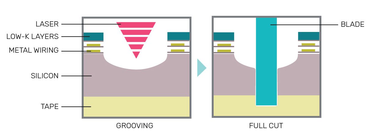
Laser grooving is therefore now the primary choice for manufacturers looking to improve the quality of wafer dicing. But even this process is not free from drawbacks. The laser itself is a complex system that needs to be positioned and repositioned accurately over the wafer to ensure it grooves along the correct point. The groove itself must be extremely precise and conform to the shape and tolerance set by the manufacturer. A groove that does not meet this tolerance can result in an improperly die cut, which is not fit for use and must be discarded. A significant amount of time must be spent by an operator using a microscope to analyze the tolerances of the grooves and clear it for dicing.
Using Vision PE microscope system, Clemex has developed a new method of automating the analysis of distance between the groove and the edge of the die.
First the wafer is correctly positioned under the lens. This is done by using a reference point and then adjusting the whole wafer so it is correctly orientated. Once this is achieved, each of the dies at the extremities or center points of the wafer will be correctly analyzed.
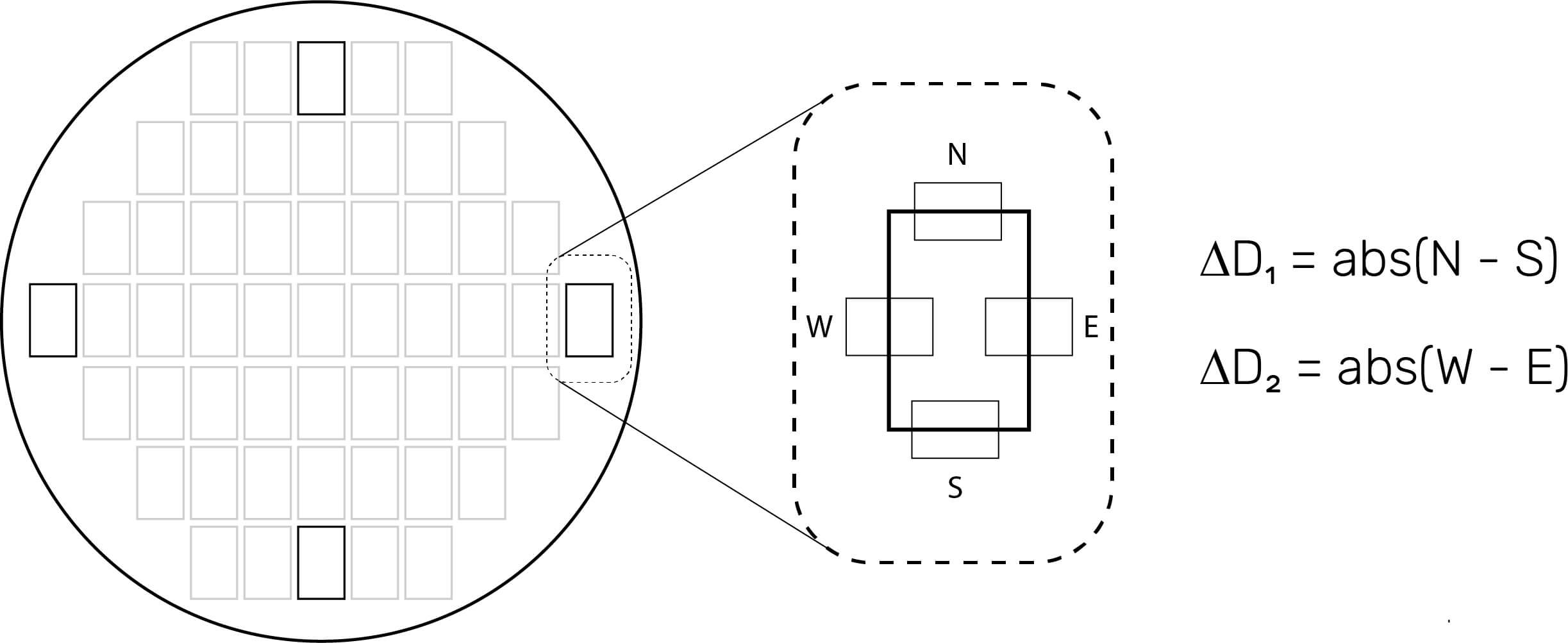
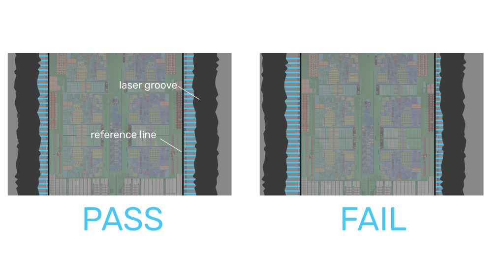
After analysis of the reference points, the laser groove itself could be analyzed. This is done by using a reference line that had been drawn around the die, and measuring the mean distance from this line to the groove itself. As this distance can vary slightly, a mean distance ΔD is taken.
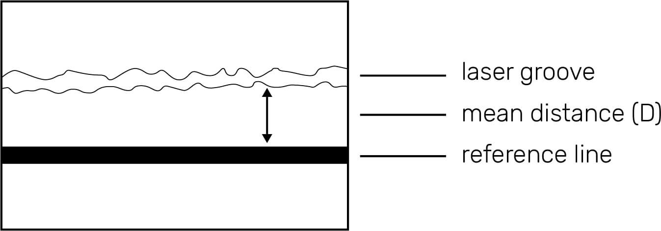
To get an overall mean distance, the absolute distance of the north edge of the die is subtracted from that of the south edge, to form an difference of distances: ΔD1. The same procedure is applied to the east and west edges to get ΔD2. ΔD values closest to 0 are best, with tolerances that form a pass-fail threshold.
If either of ΔD1 or ΔD2 are above the tolerance that is required to remove the die, then the laser grooving processes need to be reviewed. The grooving process hasn’t worked as intended, and the die cannot be removed unscathed.
This process is repeated for all of the dies on the wafer, all while working within a time constraint, with the analysis a success thanks to the extreme customizability afforded by the Vision PE. The entire program makes use of conditional statements, automatic centering, moving from target to target, and getting a clear and focused image from large distances. This can be tricky to do when the silicon wafer is up to 12 inches in diameter.
Currently, chip manufacturers are relying on human operators to manually move around the wafer and visually assess the tolerance. This process is incredibly time consuming, and prone to human error, but there hasn’t been any alternative until now. The process described here, using the Vision PE system’s excellent suite of features, means that for manufacturers are finally able to automate their analysis of laser grooving placement on a silicon wafer.
References
“Laser Grooving Characterization for Dicing Defects Reduction and its Challenges” – Koh Wen Shi, Lau Teck Beng, Yow K.Y., 11th Electronics Packaging Technology Conference, 2009
Available at:https://ieeexplore.ieee.org/stamp/stamp.jsp?tp=&arnumber=5416427
“Micro-grooving of silicon wafer by Nd:YAG laser beam Machining” – Sherpa TD, Pradhan BB, International Conference on Mechanical, Materials and Renewable Energy, 2018Available at:https://iopscience.iop.org/article/10.1088/1757-899X/377/1/012219/pdf
“Laser grooving of semiconductor wafers: comparing a simplified numerical approach with experiments” –
van Soestbergen M, Zaal JJM, Swartjes FHM, Janssen JHJ, 16th International Conference on Thermal, Mechanical and Multi-Physics Simulation and Experiments in Microelectronics and Microsystems, 2015
Available at: https://ieeexplore.ieee.org/stamp/stamp.jsp?tp=&arnumber=7103120
“Methods of Laser Dicing”
Available at: https://www.disco.co.jp/eg/laser/method.html
“The Application of Laser in WLCSP Process”
Available at: http://www.semicontaiwan.org/en/sites/semicontaiwan.org/files/data16/docs/1%20-%20The%20Application%20of%20Laser%20in%20WLCSP%20Process-final-Amkor.pdf